The Raspberry Pico is a new microcontroller launched in February 2021. The community was excited about this new board, and several people started amazing projects. I grabbed two boards early on, and while still working on my Arduino based robot, did the usual blinking led and potentiometer tutorials.
Eventually, I became more interested into the Pico, and started a new project: A library for connecting and controlling the HC595N shift register. The HC595N shift register is connected by three input pins. It receives serial data and outputs parallel data to 8 pins. In this article, I explain the fundamentals of shift registers, then detail the HC595N chip, and provide the libraries base design, its object and functions.
Shift Register Essentials
Microcontrollers allow interfacing with other peripherals through their GPIO pins: You apply binary voltage levels, high or low, or use a PWM to transmit digital data. In complex projects where you want to connect multiple peripherals to one microcontroller, the number of GPIO pins can be a limiting factor. For this, you can work with a shift register, a special device that accepts inputs and transforms them to output.
Integrated circuits consist of logic gates. Simple logic gates like AND, OR, NAND, NOR, XOR help to control the input-output processing between two devices. More complex logical devices can be grouped into combinatorial logic and sequential logic.
In combinatorial logic, input signals from one device are applied simultaneously to produce an output signal. For multiple-in, single-out translation you use multiplexer. For single-in, multiple out translations you used demultiplexer.
In sequential logic, the same principles are applied, but the signals can be relayed in time. In other words, sequential logic allows to define a logic state, and then transmit it to output with a timing mechanism. These devices are called shift register.
Shift registers can process serial or parallel input to serial and parallel output. They are controlled by input pins, which set values to the registers, and the latch and clock pins, which determine how and when the stat is transmitted to its connected output. Internally, the registers are realized by flip-flops connected in such a way that the output of one becomes the input of the next. The flip-flops are the registers. When the clock signal is applied, they will shift their current state to the next one.
The most common type of shift register translates serial in to serial out or parallel out. This type is abbreviated as SISO/SIPO, and it helps to extend the effective number of pins by controlling several output pins with just one input pin.
The HC595 Shift Register
The HC595N is an 8-BIT SIPO shift register by Texas Instrument. It is a staple shift register that might be very well working in your day-to-day use electronics or the shields/hats of your MCUs.
Let’s explore first the pin layout, then its basic operations.
Pin Layout
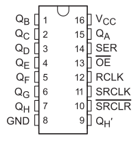
By looking at the datasheet, we see the effective pin layout as follows.
 Source: https://www.ti.com/lit/gpn/SN74HC595
Basics
- Pin 8: GN
- Pin 13: Output Enable, Active High
- Pin 16: VCC 2V ~ 6V
Input
- Pin 14: Serial (SER)
- Pin 11: Serial Clock (SRCLK)
- Pin 10: Serial Clear (SRCLR) / Active High
- Pin 12: Register Clock (RCLK)
Output
- Pin 15: QA
- Pin 1: QB
- Pin 2: QB
- Pin 3: QC
- Pin 4: QD
- Pin 5: QF
- Pin 6: QG
- Pin 7: QH
- Pin 9: QH* Serial Data Output, used for daisy chaining multiple shift registers
Operational Mode
The shift register provides the following functions:
- Serial Data In: When SRCLK goes high, and SER is High, write binary 1. If SRCLK goes high, and SER is low, write binary 0 int the first register
- Parallel Data Out: Write the current contents of the shift registers to the storage register when SRCLK goes low and RCLK goes high for 1 clock cycle
- Reset Shift Register Data: SRCLR is set to low for 2 clock cycles
- Reset Storage Register Data:
Another detail in the data sheet, that I deemed important during preparation, are the timing values when sending signals to the shift register chip. The timings differ for the applied voltages. I could not see concrete values for the 3.3V output that the rp2040 Pico provides, so these values correspond to the lower range value of 2V:
- tclock frequency: max 5Hz
- tw pulse duration: min 100Hz
Library Design
With this information, we can start to design the library. I will first discuss the main objects of the library, and then define its functions.
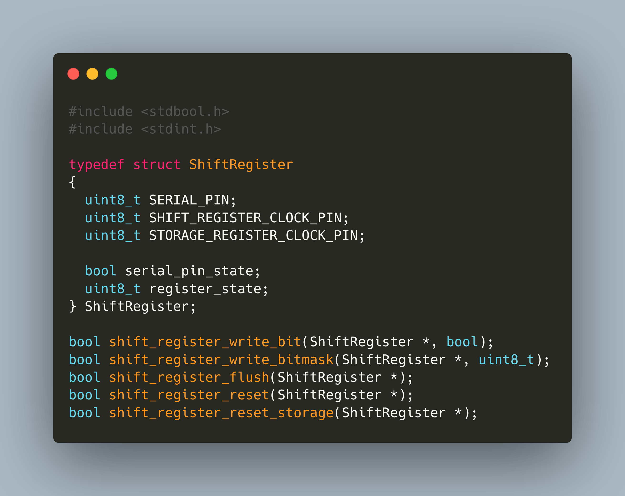
The library shall provide a single object that represents the shift register chip. This object is a C Struct. It holds the pin configuration that is used for connecting the shift register with a Pico. And it also holds two states: The current input on the serial pin, and an 8-bit integer value that represents the storage register value.
typedef struct ShiftRegister
{
  uint8_t SERIAL_PIN;
  uint8_t SHIFT_REGISTER_CLOCK_PIN;
  uint8_t STORAGE_REGISTER_CLOCK_PIN;

  bool serial_pin_state;
  uint8_t register_state;
} ShiftRegister;
This object shall provide the following functions:
- Write a single bit: Add a single bit to the first register, shifting the values of the other registers
- Write a bitmask: Set all shift register values according to a bitmask, an 8-bit integer values that can be represented in C as
0b1100110 - Flush: Transfer the current state of the shift register to the storage register, and output these values on the shift register output pins
- Reset Shift Register: Clear all values in the shift register
- Reset Storage Register: Clear all values in the storage register
These functions are defined with the following signatures:
bool shift_register_write_bit(ShiftRegister *, bool);
bool shift_register_write_bitmask(ShiftRegister *, uint8_t);
bool shift_register_flush(ShiftRegister *);
bool shift_register_reset(ShiftRegister *);
bool shift_register_reset_storage(ShiftRegister *);
With these design considerations, we can continue the library implementation in the next article.
Conclusion
Shift registers are helpful integrated circuits that receive serial or parallel data, store them, and output them again as serial or parallel data. A common shift register chip is the HC595N which provides 8-BIT serial-in, parallel out data transmission. The article explained the pin layout of this chip and its basic operations: input serial data, output parallel data, and resetting the shift register or the storage register. Based on this understanding, I provided the design fundamentals of a C library: The struct object that represents the shift library, and functions that implement the shift register operations.
In the next article we will see the library implementation.
